
Products
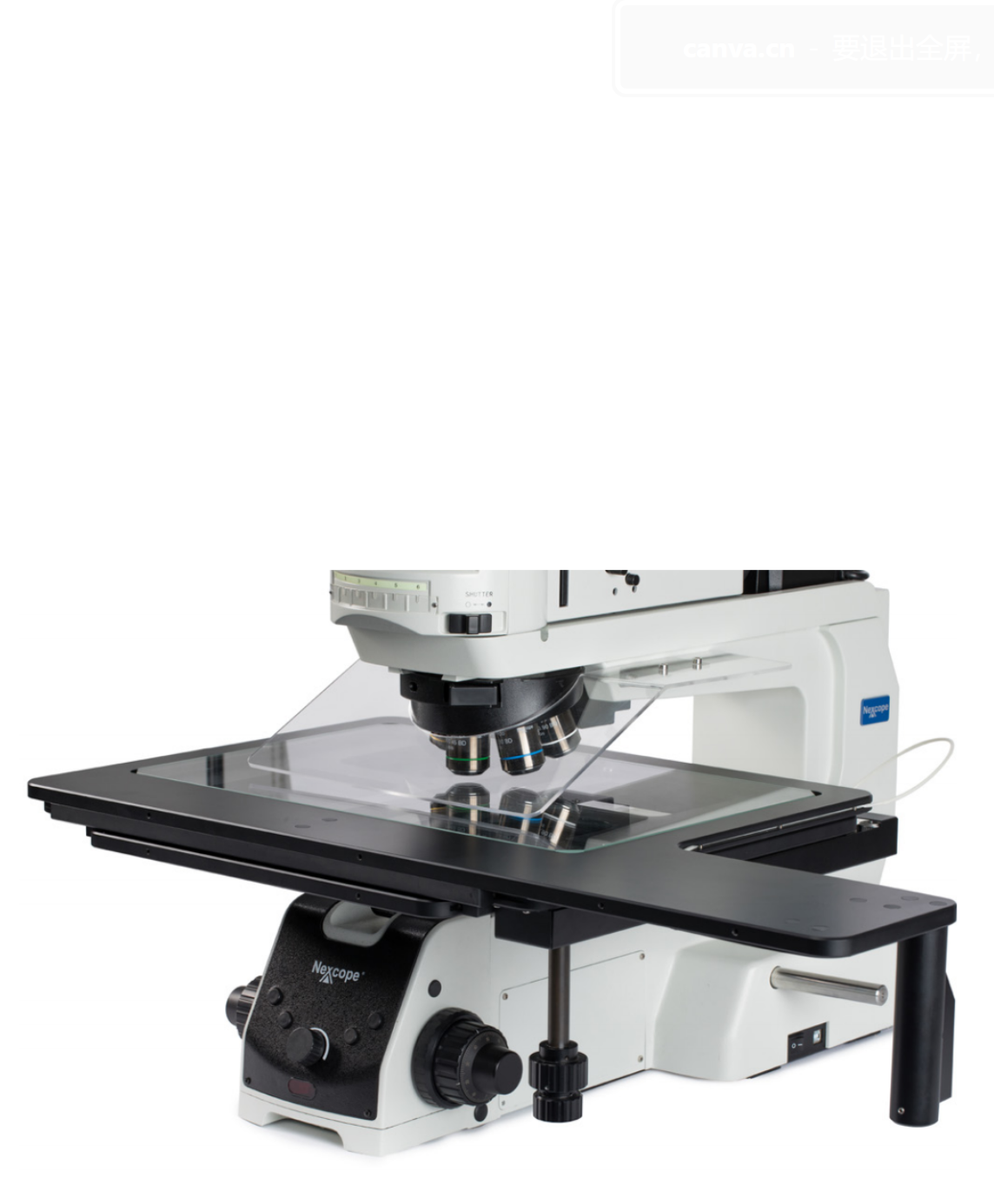
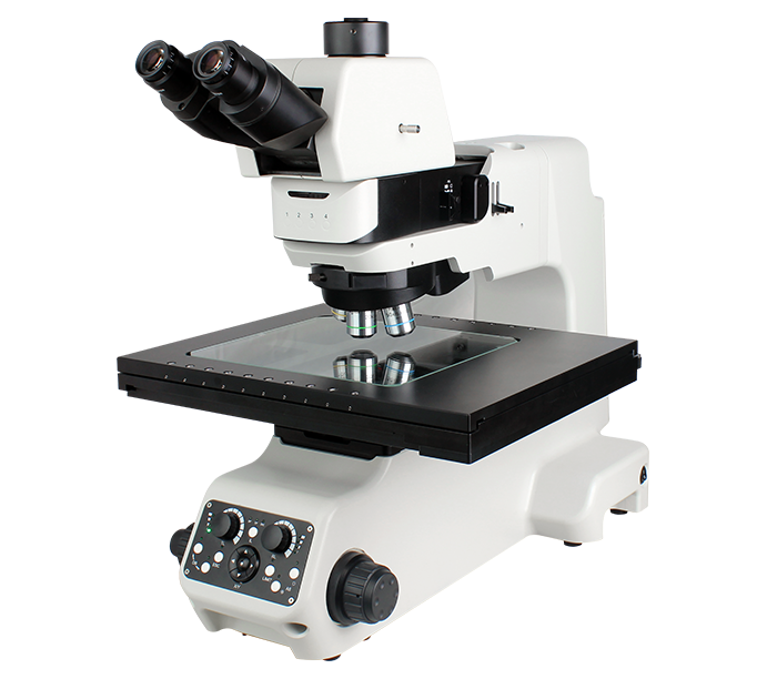
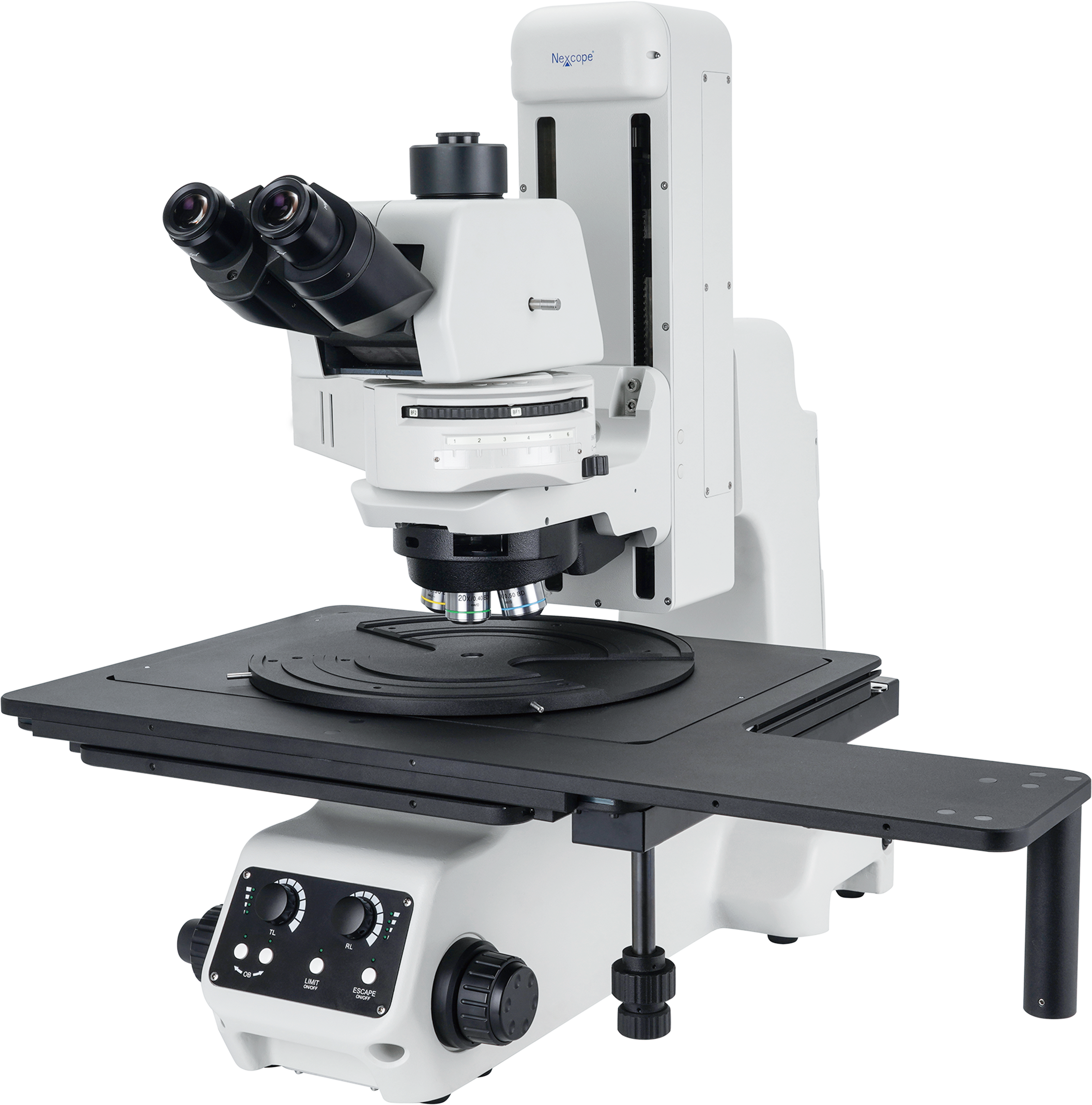
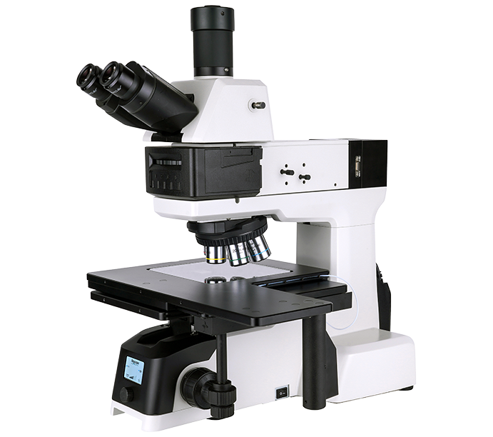
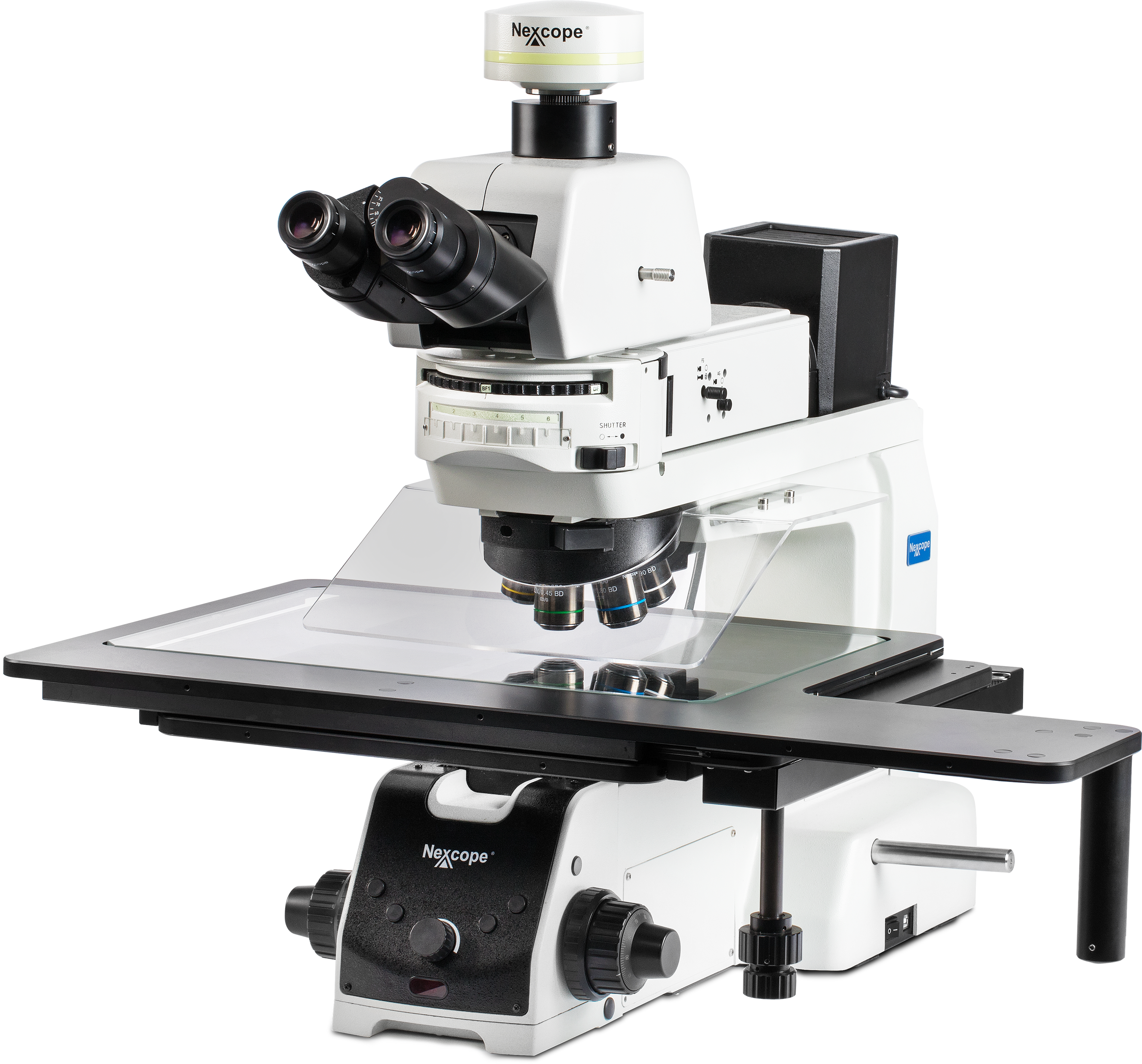
Optimized for microelectronics and semiconductor inspection. Frequently‑used controls are positioned close to the operator for fast, convenient adjustments during observation. Supplied with an erect‑image tube, delivering better synchronization between stage movement and viewing compared with traditional inverted‑image tubes.
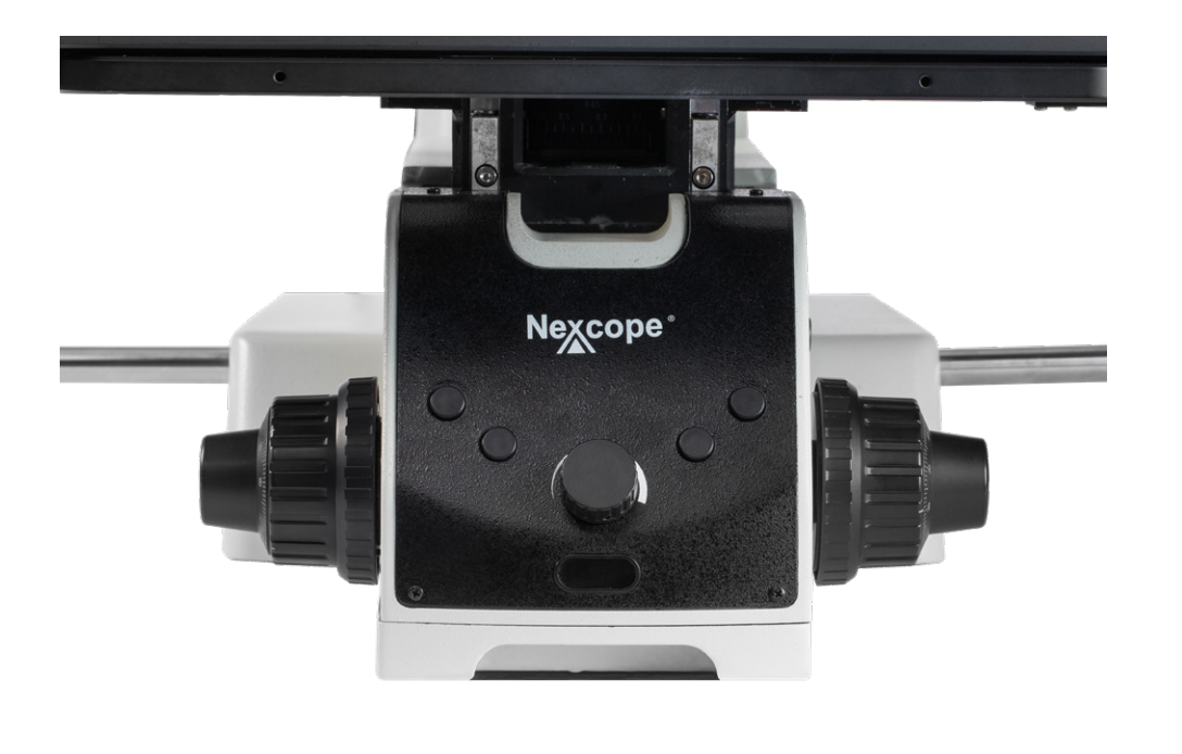
Clutch-Equipped Stage Handle
Fast and slow movement modes for large-area positioning. Paired with fine-adjust handle for precise, quick sample location.

Built-In Control Panel
Buttons mapped to specific objectives — one press changes magnification.

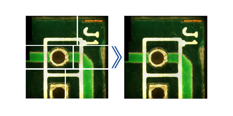
Image stitching

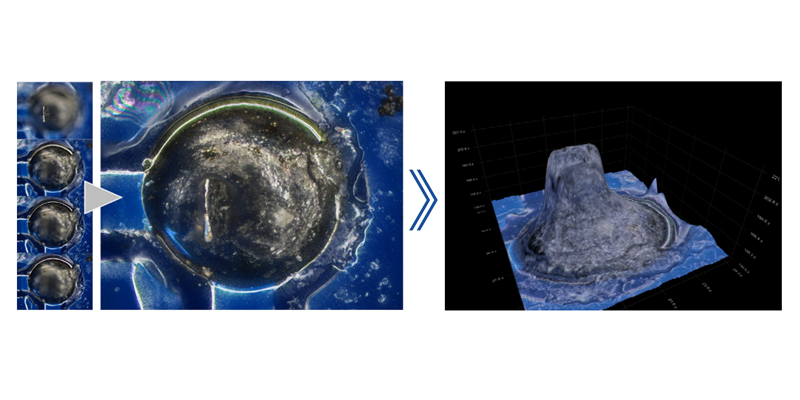
Depth-of-field fusion / 3D reconstruction

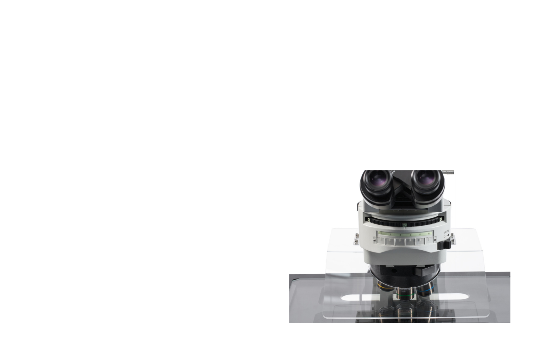
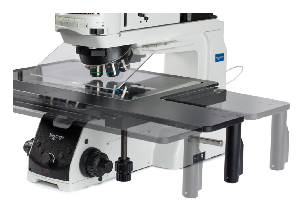
Oversized Stage
Microelectronics and semiconductor samples are often large; conventional metallographic stages fall short. NX1000 offers oversized stage and travel with smooth movement — ideal for large-area industrial inspection.

Anti-Static Dust Shield
Industrial samples are dust-sensitive. Large anti-static protective cover.

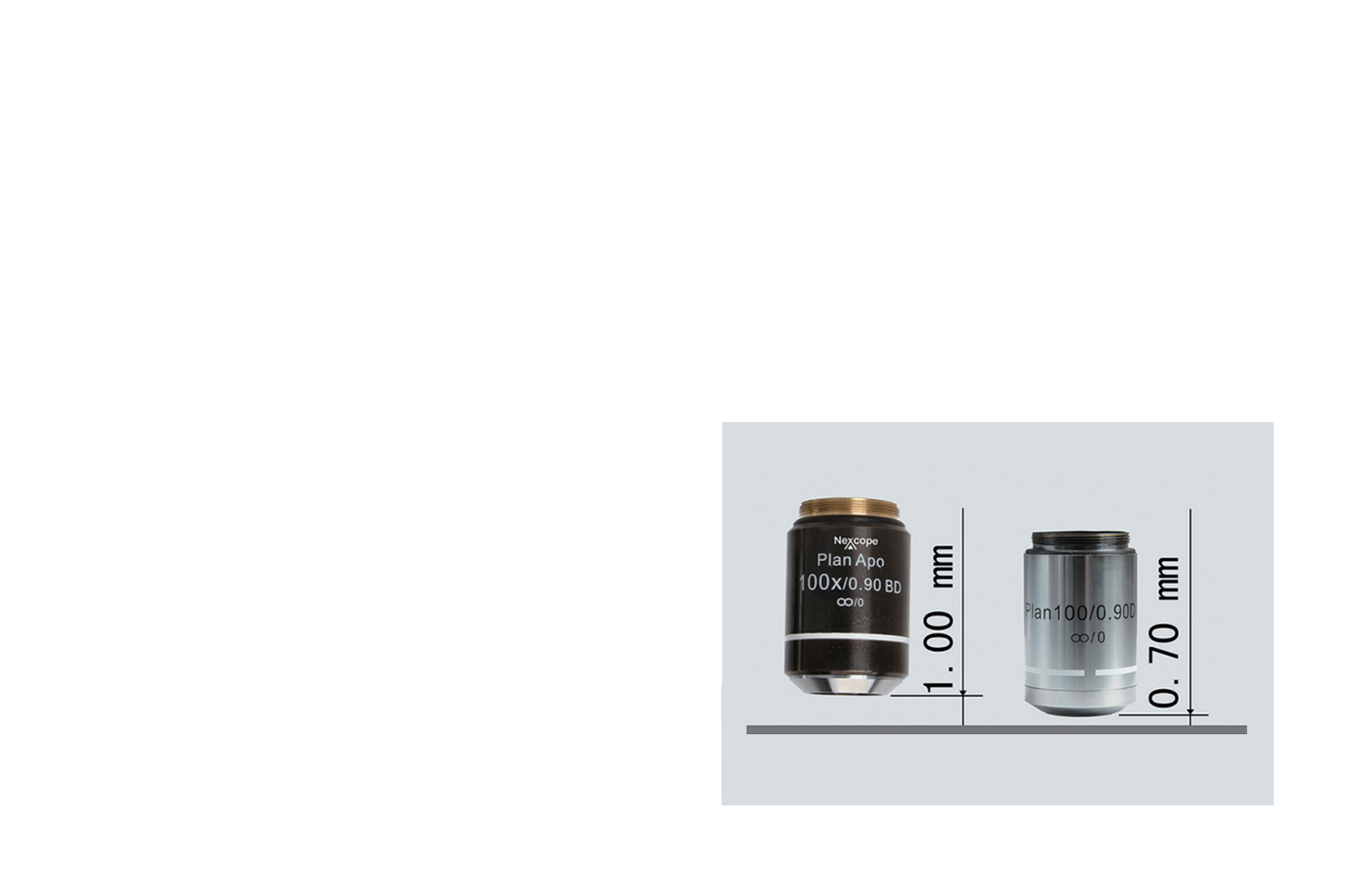
Long-WD, High-NA Objectives
Electronic components and semiconductors create large height differences on circuit boards — dedicated long-WD objectives.

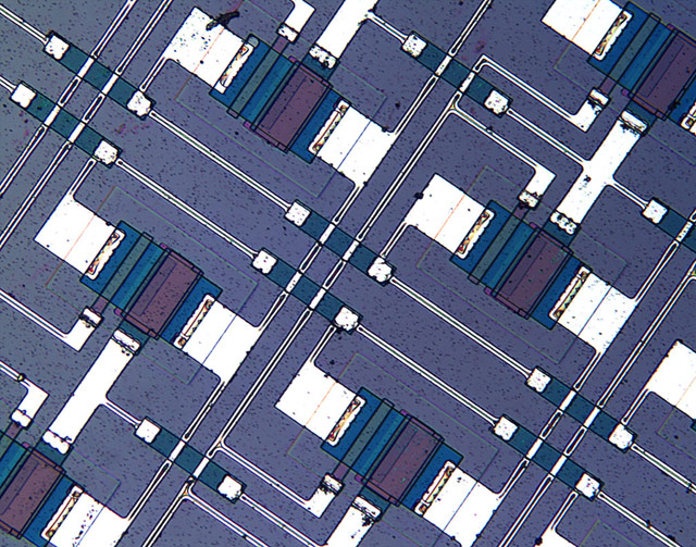
Epi-Brightfield
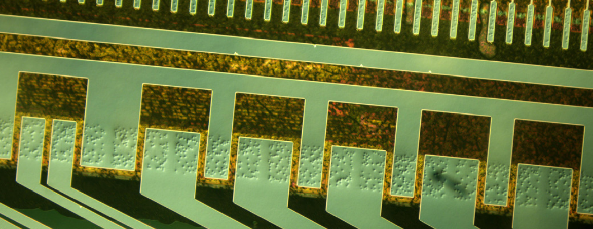
NIS infinity-corrected system. Uniform, bright, high-color-fidelity viewing. For opaque samples such as semiconductors.

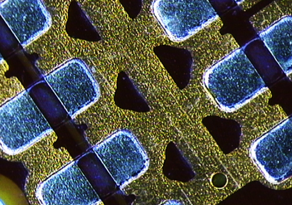
Darkfield
Bright darkfield observation for high-sensitivity detection of fine scratches and defects. For high-spec surface inspection.

Transmitted Brightfield
For transparent samples (FPD, optical components) via transmitted-light condenser. Also pairs with DIC and simple polarization.

Simple Polarization
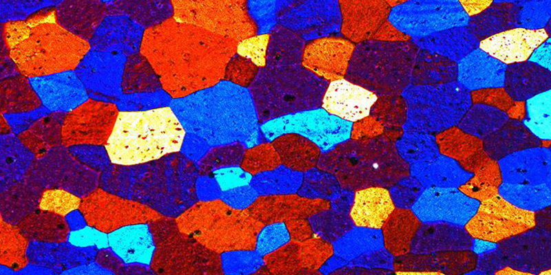
For birefringent specimens: metallographic structures, minerals, LCD, semiconductor materials.

Epi-DIC
Reveals fine height differences in precision molds as relief and 3D imagery.

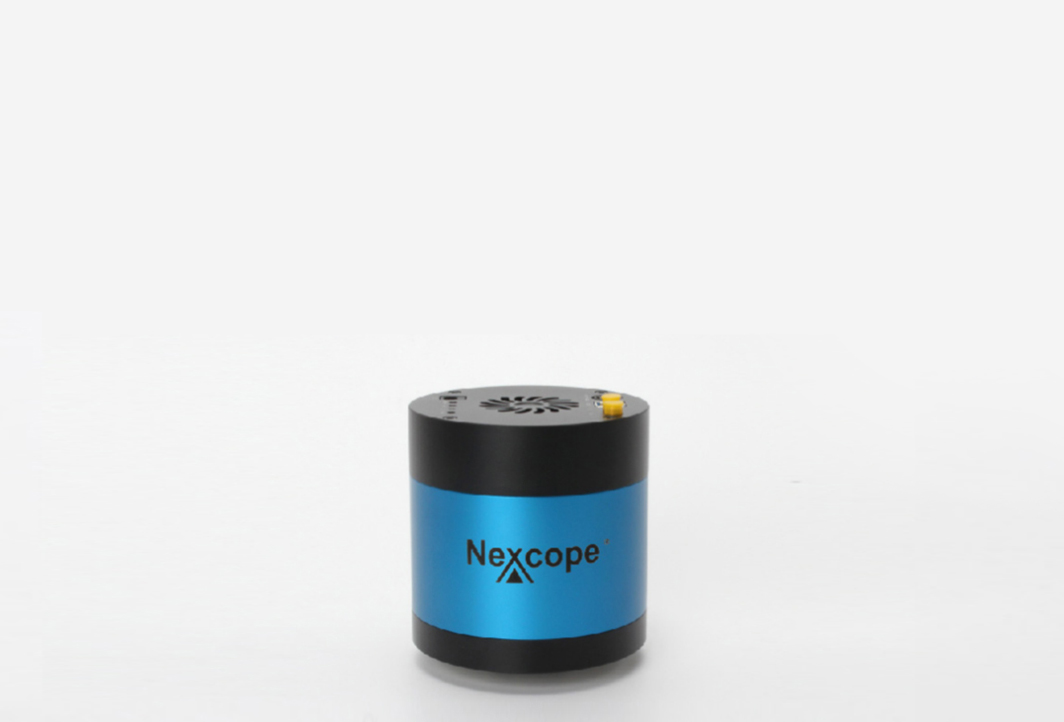
TC6CCD
1‑inch, 6‑megapixel CCD

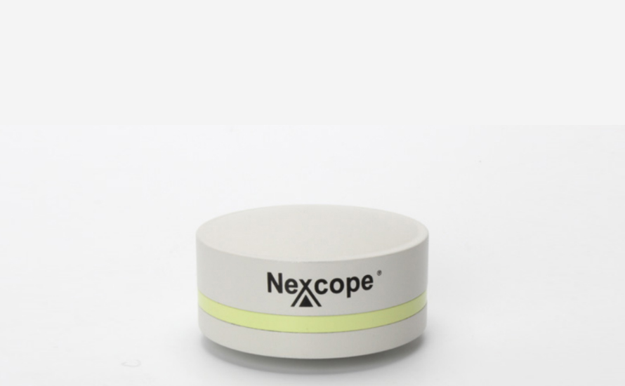
T6CCD
1‑inch, 6‑megapixel CCD

T16
4/3‑inch, 16‑megapixel CMOS